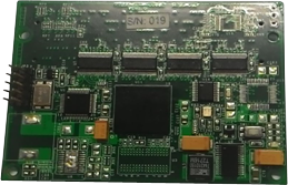
A generic System on Module built using Atmel AT91SAM9263 Processor running at 200 MHz. The card provides basic standard interfaces as shown in the block diagram. The LV-SOM module connects to a Printed Circuit Board (PCB) through two 240-pin board-to-board (BTB) connectors. All the signals from LV-SOM are routed to two BTH 240-pin connectors.
The SOM has 64Mbytes of System memory implemented using two SDRAMs, a NAND Flash of 256 Mbytes, a NOR Flash of 8MBytes and a Serial EEPROM of 512Kbits, SRAM of 4MB as LCD Frame Buffer. This Card Boot-up can be either from Internal ROM, NAND Flash, NOR Flash or SPI Serial EEPROM.
Taking advantage of a rich set of peripheral available on-chip the card provides for all the required serial ports, Ethernet ports, Keypad port, LCD port and USB ports. A 4x4 matrix keypad can be interfaced to the card using on-chip keypad scanner. A monochrome STN LCD or Color TFT LCD can be interfaced using an on-chip LCD controller. A full speed Ethernet Port is provided with an on-chip MAC plus external PHY device and the AC97 Controller. The card also supports two SPI 2 wire Interfaces, one JTAG/ICE debug interface, one CAN Bus Port, two SDCard/SDIO and Multimedia Card Compliant ports and 4X4 matrix Keypad Interface.
There is an on-board Xilinx XC9500 CPLD, which is customizable to handle various digital IOs and glue logic. A separate JTAG connector is provided for programming and downloading of configuration files to the CPLD.
The card works from a single +3.3V power supply and all the internal Voltages required by various other peripherals are derived using on board regulators and DC-DC Converters.
The card has been designed as a System on Module confirming to SOM-LV form factor and can be used in most of the applications requiring such a medium sized processor with common interfaces.
The further sections of the document, explain in detail the different blocks of the card.
|