SERVICE & SOLUTIONS > CUSTOM PRODUCT DEVELOPMENT > DIGITAL / ANALOG PRODUCTS > CPU BOARD
  • Features
  • Overview
 
Embedded single-issue, 32-bit MPC8xx core (implementing the PowerPC architecture) with thirty-two 32-bit general-purpose registers (GPRs)
> The core performs branch prediction with conditional prefetch, without conditional execution
> 4- or 8-Kbyte data cache and 4- or 16-Kbyte instruction cache
> MMUs with 32 entry TLB, fully associative instruction and data TLBs
> MMUs support multiple page sizes of 4, 16, and 512 Kbytes, and 8 Mbytes; 16 virtual address spaces and 16 protection groups
> Advanced on-chip-emulation debug mode
Up to 32-bit data bus (dynamic bus sizing for 8, 16, and 32 bits)
32 Address lines
Operates at up to 80 MHz
Memory controller (eight banks)
> Contains complete dynamic RAM (DRAM) controller
> Each bank can be a chip select or RAS to support a DRAM bank
> Up to 15 wait states programmable per memory bank
> Glueless interface to DRAM, SIMMS, SRAM, EPROM, Flash EPROM, and other memory devices.
> DRAM controller programmable to support most size and speed memory interfaces
> Four CAS lines, four WE lines, one OE line
> Boot chip-select available at reset (options for 8-, 16-, or 32-bit memory)
> Variable block sizes (32 Kbytes to 256 MBytes)
> electable write protection
> On-chip bus arbitration logic
Four 16-bit timers or two 32-bit General Purpose timers
Software watchdog and real-time clock
IEEE 1149.1 test access port (JTAG)
10/100 Mbps Ethernet support, fully compliant with the IEEE 802.3u Standard
Communications processor module (CPM)
> RISC communications processor (CP)
> Up to 8Kbytes of dual-port RAM
> 16 serial DMA (SDMA) channels
Four baud-rate generators (BRGs)
Four serial communications controllers (SCCs)
One SPI (serial peripheral interface)
One I2C (inter-integrated circuit) port
Debug interface: Eight comparators: four operate on instruction address, two operate on data address, and two operate on data

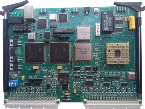
The CPU board is designed around the PowerPC processor MPC860T from Freescale semiconductor

The MPC860 Quad Integrated Communications Controller (PowerQUICC™) is a versatile one-chip integrated microprocessor and peripheral combination that can be used in a variety of controller applications. It particularly excels in both Communications and networking systems. The MPC860 is a derivative of Motorola’s MC68360 Quad Integrated Communications Controller (QUICC™), referred to here as the QUICC, which implements the PowerPC architecture. The CPU on the MPC860 is a 32-bit MPC8xx core implementation that incorporates memory management units (MMUs) and instruction and data caches and that implements the PowePC instruction set. The memory controller has been enhanced, enabling the MPC860 to support any type of memory, including high-performance memories and new types of DRAMs.

The MPC860T processor is mainly used in the RADAR Systems (Bharani and Rohini Radar)

MPC860T processor integrates the enhanced PowerPC core and advanced features such as SDRAM with 1GB, 128 MB of NOR flash, 8GB of NAND Flash, up to 1 GHz of clock speed, up to 16MB of NVRAM. The system provides the required interfaces to interface custom modules in the system. The system provides communication bus interfaces like asynchronous communication port on RS232 and two-gigabit Ethernet ports

Field Programmable Gate Array used is Defense-grade Virtex®-7Q device that offers the largest portfolio of high-performance, high reliability for systems in markets such as Intelligence, Surveillance and Reconnaissance (ISR), Electronic Warfare (EW), Commercial & Military Avionics

On-board it has 512Kx32 FLASH MODULE, In-System Programmable CPLD which has 36 macrocells with 800 usable gates, High performance 32K x 8 Static RAM, 16k Nonvolatile SRAM, HIGH-SPEED 64K x 8 DUAL-PORT STATIC RAM, In-System Programmable Configuration PROM

ARINC429 Interface
Type II PC Card
16 bit PCMCIA Architecture
DDC Controller
2Tx / 4Rx ARINC429 Channel
128 x 32 bit Static RAM interface
Programmable Interrupts
Configurable Bit Format Control
Built-in Fault Detection Circuitry
Transmit Interface
Programmable 12.5/100KHz bit rate
Two 32 (words deep) x 32 (bit) Transmit FIFO’s
Independent data transmit by each channel
Programmable data transmit rate for each channel
Transmit FIFO Status Indicators
Receive Interface
Four 32 (words deep) x 32 (bit) Receive FIFO’s
Receive data rates can be programmed for channel 0 and 1 independent of channel 2 and 3 in each ARINC429 controller
Reducing Receive Data Latency
Filtering & Sorting of data
Storage of data
Parity Error Checking & Reporting
Receive FIFO status indicator
Diagnostics
Testing of Memory Elements
Testing Transmit/Receive functions
Wraparound Test for each channel
Interrupt Function Testing
Error Conditions
Sequence Error
Address Error
FIFO Overflow Error
Receive Data Parity Error
ARINC Clock Error
Software Support
Driver and high-level API libraries for Windows XP
A powerful 'Virtual Instrument Panel' developed to mimic the physical card features & capabilities for interactive control & monitoring
Sample applications provided
Physical
Type II PC Card
Card dimensions- 54.0 x 85.6 x 5 mm
Environmental
Operating temperature: 0º C to +50º C
Storage temperature: -20º C to +70º C
Power
+ 5 VDC
Warranty
1 year limited warranty
 
CORPORATE   ABOUT   FOLLOW US ON
AdTEC Electronics Inc.
4677 Old Ironsides Drive
Ste 230 Santa Clara
California 95054, USA
 
AdTEC Electronics specializes in providing end-to-end custom product design & development encompassing System, Mechanical, Board Electronics, Chip design, Firmware and Application Software Engineering. Our design capabilities include design for testability and rugged design to meet both commercial and stringent regulations.
 
HOME ABOUT US COTS PRODUCTS SERVICES & SOLUTIONS SUPPORT & RESOURCES NEWS & EVENTS BLOG CONTACT US
AdTEC Electronics Inc.